您的购物车目前是空的!
标签: USRP
-
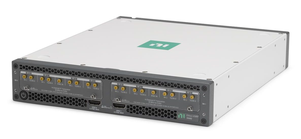
USRP X440
788670-01 | ETTUS USRP X440 (8 TX AND 8 RX, 1.6 GHZ BW, 30 MHZ TO 4 GHZ SDR, GPSDO) $ 29,234.00 USD
30 MHz to 4 GHz, 1.6 GHz Bandwidth, 8 TX and 8 RX, Phase-Coherent, GPS-Disciplined OCXO, USRP Software Defined Radio Device
Overview
The Ettus USRP X440 is a USRP Software Defined Radio (SDR) Device that helps you integrate hardware and software for prototyping high-performance, multichannel, wideband signal generation and analysis systems. This SDR features 8 TX and 8 RX channels with a direct sampling transceiver architecture. It also features a Xilinx Zynq UltraScale+ RFSoC with programmable FPGA supporting the open source UHD and RFNoC tool flows for integration of external up- and downconversion, filtering, and amplification front ends. With these features, the Ettus USRP X440 has the IF and processing performance for applications such as radar, EW, SATCOM and mmWave development and prototyping. Additionally, the Ettus USRP X440 includes a GPS-disciplined 10 MHz oven-controlled crystal oscillator (OCXO) Reference Clock, which improves frequency accuracy and synchronization.
Dual Rate
The Ettus USRP X440 supports being operated at two different master clock rates simultaneously. Due to the direct sampling architecture of the USRP X440, TX and RX signals are affected by Nyquist zones and their boundaries. By using different rates for both radios, one can close the Nyquist gap of the other.
Features
RF Features:
- Front End: Balun-coupled MMPX
- IF Range: 30 MHz – 4 GHz*
- Bandwidth: up to 1.6 GHz*/channel, 3.2 GHz total
- Direct Sampling: Flexible up to 4 GSps
- Channel Count: 8 (Tx/Rx or TRX)
- Phase Coherency: Yes (sample-based)
- Phase Stability (within device): < 1° RMS
- Phase Stability (device-to-device): < 2° RMS
- Phase Repeatability (within device): < 3° Peak-to-Peak
- Tx Output Level: < 0 dBm full scale
- Rx Input Level: 10 dBm full scale
* IF-Bandwidth combination limitations apply due to Nyquist zones and gaps
Digital Features:
- Xilinx Zynq UltraScale+ RFSoC ZU28DR-2
- Built-in quad-core ARM processor
- Streaming Interface: Dual 100 GEth via QSFP28
- Synchronization: 10 MHz / PPS, GPSDO, IF
- Software: Open source (GNU Radio, RFNoC, UHD)
- GPIO for front-end control via UHD API or FPGA
- 2x 12 lanes via HDMI with SPI protocol support
Quotes and Sales
Email:sales@tekdf.com
Wechat:dftech_info
-
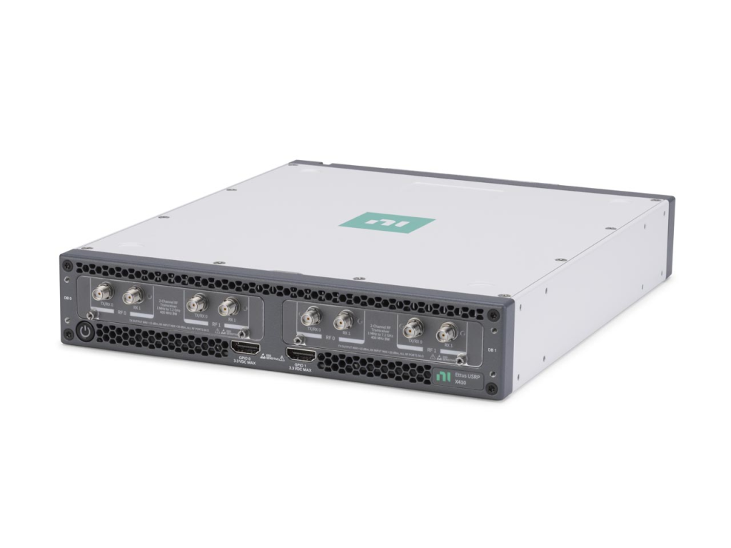
USRP X410
787272-01 | USRP X410 (4 TX/RX Channels, 400 MHz BW, Zynq US+ RFSoC ZU28DR) $ 29,950.00 USD
The NI Ettus USRP X410 is a high-performance, multi-channel, Zynq US+ RFSoC based software defined radio (SDR) for designing and deploying next generation wireless systems.
Overview
The NI Ettus USRP X410 is a high-performance, multi-channel software-defined radio. The SDR is designed for frequencies from 1 MHz to 7.2 GHz, tunable up to 8 GHz and features a two-stage superheterodyne architecture with 4 independent TX and RX channels capable of 400 MHz of instantaneous bandwidth each. Digital interfaces for data offload and control include two QSFP28 interfaces capable of 100 GbE, a PCIe Gen3 x8 [1] interface, as well standard command, control, and debug interfaces: USB-C JTAG, USB-C console, Ethernet 10/100/1000. The USRP X410 is an all-in-one device built on the Xilinx Zynq Ultrascale+ ZU28DR RF System on Chip (RFSoC) with built-in digital up and down conversion and onboard Soft-Decision Forward Error Correction (SD-FEC) IP.
Use the software of your choice
The NI Ettus USRP X410 is fully supported on the popular open-source USRP Hardware Driver (UHD) version 4.1 or later[2]. UHD 4.1 was designed to support the large data movement requirements imposed by the 400 MHz bandwidth and multiple channels onboard. The USRP X410 supports open-source SDR design flows such as C/C++ and GNU Radio, as well as LabVIEW FPGA [1]. Unlike other RFSoC-based systems, the USRP X410 is fully ready to port your previous UHD designs to take advantage of high-performance capabilities with a simple recompile.Networked / Stand-Alone Operation
Since the USRP X410 is built on the ZU28DR RF System on Chip (RFSoC) device, it comes equipped with a quad-core ARM Cortex-A53 processing subsystem, clocked up to 1.2 GHz for stand-alone application requirements. Additionally, the RFSoC contains a dual-core ARM Cortex-R5 real-time processing unit for onboard monitoring and control.Built-In IP
The onboard RFSoC on the USRP X410 contains more than twice the FPGA programmable logic resources than that of the previous generation X-series USRP devices. In addition, the ZU28DR comes with 8 soft-decision forward error correction (SD-FEC) hard IP cores, ideal for wireless communication systems. Given the high-speed nature of the built-in ADCs and DACs to the RFSoC, the Zynq device has 8 digital upconversion and digital down-conversion IP cores allowing for rapid in-band retuning or signal reduction.Multi-Radio Synchronization
Multi-radio clocking and timing synchronized operation is possible with the built-in GPSDO (GPS disciplined oscillator) or with the 10 MHz reference and 1 PPS (Pulse Per Second) input signal interfaces. Multi-Radio phase-aligned and phase-coherent operations are not supported, as RF chain LO import and export functionality is not supported on the USRP X410.[1] PCIe Gen3 x8 is only supported by NI-USRP and LabVIEW FPGA design flows
[2] 100 GBE supported in UHD 4.2 or laterFeatures
- High channel density
- Reliable and fault-tolerant deployment
- Stand-alone (embedded) or host-based (network streaming) operation
- Fully integrated and assembled (the USRP X410 does not support swappable daughtercards)
- 1 MHz to 7.2 GHz frequency range (tunable up to 8GHz)
- Up to 400 MHz of instantaneous bandwidth per channel
- 4 RX, 4 TX in half-wide RU form factor
- Xilinx Zynq-Ultrascale+ ZU28DR RFSoC
- 12 bit ADC, 14 bit DAC
- IQ Sample Clock rates up to 500 MS/s
- Onboard SD-FEC, DDC, DUC
- Quad-core ARM Cortex-A53 up to 1.2 GHz CPU
- Dual-core ARM Cortex-A5 MPCore up to 500 MHz
- Two QSFP28 ports (10 Gigabit Ethernet, 100 Gigabit Ethernet, Aurora)
- Two iPass+™ zHD® Interfaces (PCIe Gen3 x 8)
- RJ45 (1 GbE) [1]
- 10 MHz Clock reference
- PPS time reference
- Trig In/Out Interface
- Built-in GPSDO
- Two FPGA Programmable GPIO Interfaces (HDMI)
- 1 Type C USB host port
- 1 Type C USB port (serial console, JTAG)
- Watchdog timer
- OpenEmbedded Linux
- USRP Hardware Driver™ (UHD) open-source software API version 4.1.0 or later
- RF Network on Chip (RFNoC™) FPGA development framework
- Xilinx Vivado® 2019.1 Design Suite (license not included)
- GNU Radio support is maintained by Ettus Research™ through GR-UHD, an interface to UHD distributed by GNU Radio
[1] The RJ45 port is used for remote management of the device and does not support IQ streaming.
Additional Resources
Kit Contents
- USRP X410
- RJ45 Ethernet Cable
- USB-C to USB-A cable
- Power Supply
Quotes and Sales
Email:sales@tekdf.com
Wechat:dftech_info